JTAG Isolator: Difference between revisions
From Kamamilabs.com - Wiki
Anna Kubacka (talk | contribs) No edit summary |
|||
| Line 4: | Line 4: | ||
<center> | <center> | ||
[[File:jtag- | [[File:jtag-isolator_v2.jpg|none|800px|thumb|center]] | ||
</center> | </center> | ||
===== Basic parameters ===== | ===== Basic parameters ===== | ||
Revision as of 08:41, 6 February 2024

Description
JTAG Isolator is a galvanic isolator of JTAG interface, which protects from electrical damage of device. Cause of damage can be differences in reference potentials in together connected devices (e.g. computer and development board) with JTAG interface.
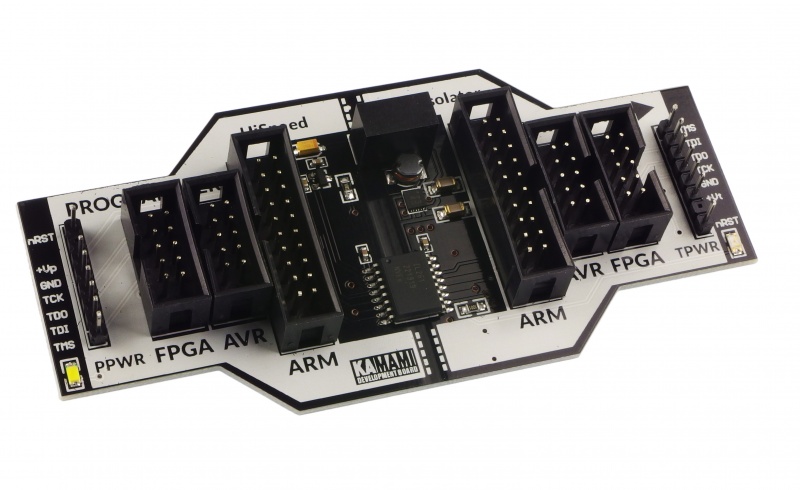
Basic parameters
- Galvanic isolation of 5-lines JTAG interface
- Max frequency TCK: 110 MHz(*)
- Power supply from target device (3...5 V)
- Compatibility with all JTAG interfaces powered by voltage 3...5 V
- Logical levels on Programmer: TTL/TTL-LV
- Logical levels on Target: TTL-LV
- Max current consumption: 50 mA
- Isolation voltage: 750 VAC/1 kVDC
- Optical signalization of power supply conntection
- Optical signalization of galvanic battery power supply
- Embedded connectors:
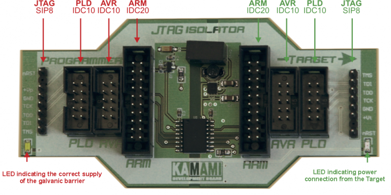
- IDC10 – JTAG for PLD (FPGA and CPLD) – complies with programmer Altera ByteBlaster, IDC10 ** JTAG for AVR microcontrollers,
- IDC20 – JTAG for ARM microcontrollers and microporcessors,
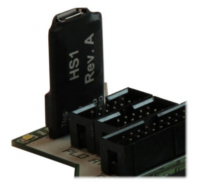
- SIP8 – JTAG for PLD (FPGA and CPLD) – complies with programmer Digilent JTAG HS1.
- Current consumption from +Vp line for programmer: max 10 mA
(*) It depends on length of connection cables
| Output on Separator and Target area can’t be connected together or touched at the same time – they can be in different potentials which may result in electric shock or damage of the device. |
Standard equipment
| Code | Description |
|---|---|
| JTAG Isolator |
|
Placement of the most important components
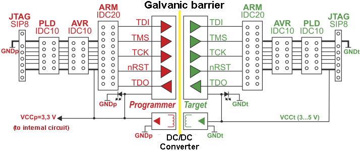
Block schematic
Power supply of separator
Both electric area (Target i Programmer) of separator are powered from Target side. Electric energy for Programmer side are provided from embedded in device, galvanic isolated DC/DC converter. For this reason, it is necessary to provide an additional current supplying of the separator, the value of which depends on the supply voltage (as in the table below). The programmer connected on the “Programmer” side should be powered from a separate source, it is allowed to supply only the I/O buffers from the + Vp line of the separator. The maximum load capacity of the + Vp line is 10 mA @ 3.3 V.
Current consumption by separator on Target side
| Voltage +Vt [V] | Current consumption on +Vt [mA |
|---|---|
| 3 | <50 |
| 3,3 | <45 |
| 4 | <30 |
| 5 | <35 |
Allowed logical levels
Separator from Target side can be powered by voltage from Vt = 3 to Vt = 5 V. Levels acceptable voltages on output and input lines are from 0 V to Vt, wherein low level valtage „0” are from 0 to 0,8 V, and for „1” are 2,4...Vt. On Programmer side it is recommended to include programming interfaces with buffers I/O powered by voltage Vp = 3,3 V. Range of logical „0” are 0...0,8 V, and for „1” are 2,4...Vp. Exceeding the voltage level on Programmer side on I/O lines over Vp can damage a separator.
Connection for AVR
Separator from Target can be powered by voltage from Vt = 3 do Vt = 5 V. Levels acceptable voltages on output and input lines are from 0 V to Vt, wherein low level voltage „0” are from 0 to 0,8 V, and for „1” are 2,4...Vt. On Programmer side it is recommended to include programming interfaces with buffers I/O powered by voltage Vp = 3,3 V. Range of logical „0” are 0...0,8 V, and for „1” are 2,4...Vp. Exceeding the voltage level on Programmer side on I/O lines over Vp can damage a separator.
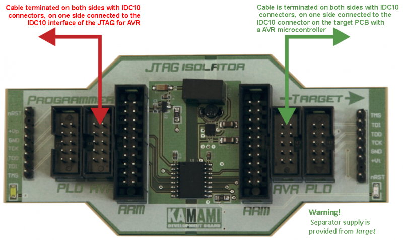
| Maximum frequency of TCK can be 110 MHz. It depends on length of connection cables and PCB wires (the longer it is, the lower is fTCKmax) and kind of load on each I/O lines on Target side. |
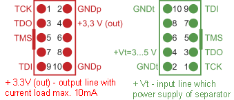
Description of signals for AVR connector on Programmer side (red) and Target (green).
Connection for ARM
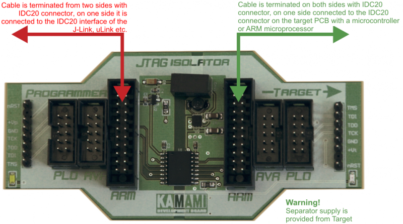
The way of using the JTAG separator Isolator for programming/debugging system with ARM microcontroller.
| Maximum frequency of TCK can be 110 MHz. It depends on length of connection cables and PCB wires (the longer it is, the lower is fTCKmax) and kind of load on each I/O lines on Target side. |
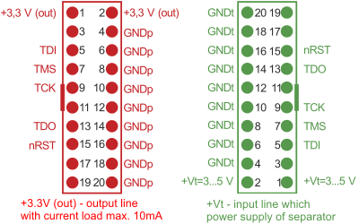
Description of signals for ARM connector on Programmer side (red) and Target (green).
Connection for PLD (CPLD/FPGA)
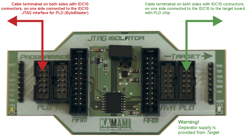
| Maximum frequency of TCK can be 110 MHz. It depends on length of connection cables and PCB wires (the longer it is, the lower is fTCKmax) and kind of load on each I/O lines on Target side. |
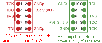
Description of signals for PLD (compatible with ByteBlaster) connector on Programmer side (red) and Target (green).
Connection for any JTAG
Separator is equipped with SIP8 goldpin connector with pins 2,54 mm, to which you can attach any JTAG interfaces or other ones that require galvanic separation.
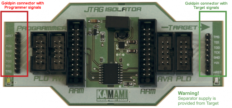
The placement of signals on the pin connectors make possible to install on them the Digilent JTAG HS1 programmer-configurator (see photo below).
