ZL10PLD: Difference between revisions
From Kamamilabs.com - Wiki
Anna Kubacka (talk | contribs) No edit summary |
m Text replacement - "__jzpdf__" to "__jzXpdf__" |
||
| Line 1: | Line 1: | ||
__jzXpdf__ | |||
===== Description ===== | ===== Description ===== | ||
The dipPLD modules are designed to helps using of Spartan 3 FPGA devices by people that can’t use automatic assembly of QFP packages. | The dipPLD modules are designed to helps using of Spartan 3 FPGA devices by people that can’t use automatic assembly of QFP packages. | ||
Revision as of 00:53, 30 October 2024
__jzXpdf__
Description
The dipPLD modules are designed to helps using of Spartan 3 FPGA devices by people that can’t use automatic assembly of QFP packages.
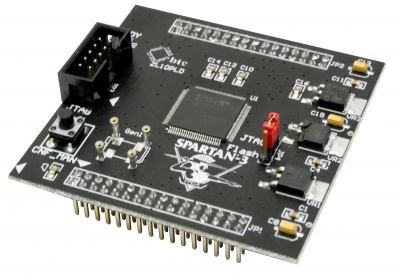
Key features
- XC3S200 Spartan 3 FPGA device in VQFP100 package (equivalent for 200000 logic gates, 12 hardware multipliers, 4 frequency multipliers, 216kb of Block SRAM)
- flash configuration memory size: 1Mb (XCF01S)
- 61 I/O lines (including five 5V-tolerant input lines)
- built-in LVC/LCX inverters for buffering 6 I/O lines
- switch for manual configuring FPGA
- LED indicating correctly configured FPGA
- JTAG interface (ZL11PRG, ZL11PRG-M or ZL4PRG)
- quartz generator 3.6864 MHz
- built-in voltage regulators: 1.2/2.5 and 3.3V
- 4.4–7VDC power supply
- current consumption: 110mA (depend on frequency)
- ready to use with ZL9PLD base board
| For ZL10PLD dipPLD module are available free PCB and SCH libraries for Protel99SE and Protel DXP. They can be downloaded from: https://download.kamami.pl/p29367-zl10pld_libs.zip |
ZL10PLD module works with ZL9PLD base board. 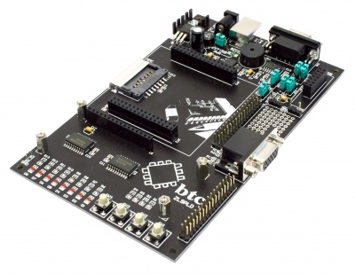 |
Standard equipment
| Code | Description |
|---|---|
| ZL10PLD |
|
Module configuration
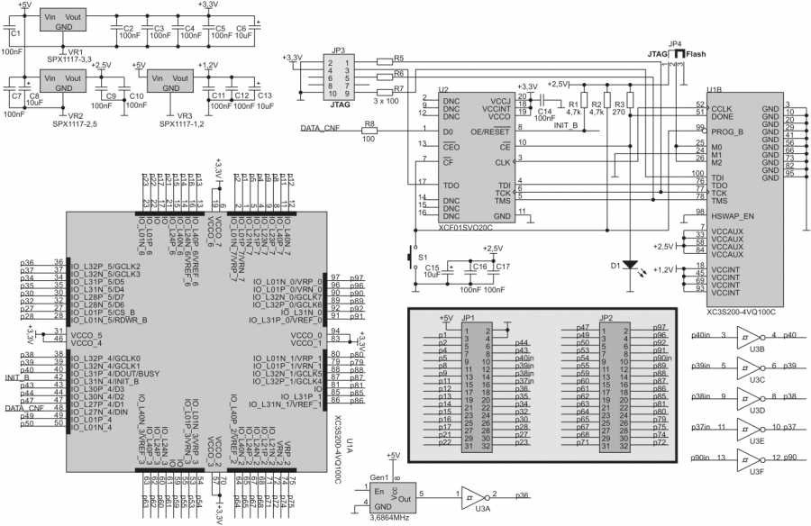
Electrical schematic of ZL10PLD is shown in the below picture.
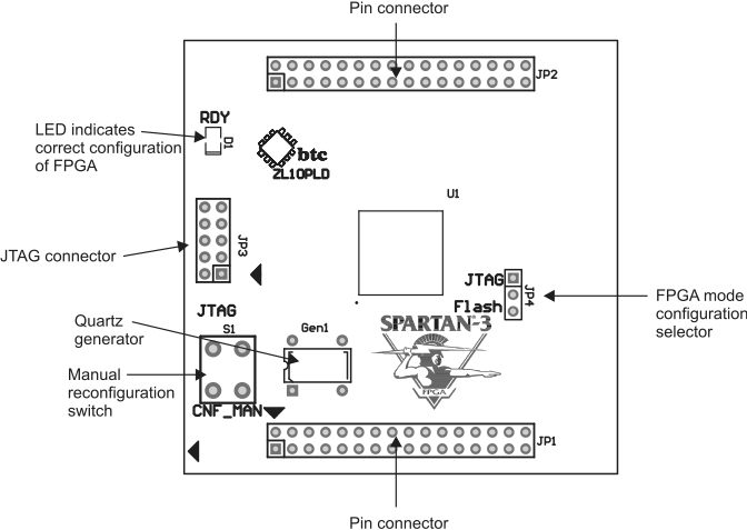
Arrangement of the most important module
Module pins
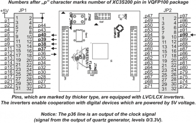
| I/O line, marked by „p36” symbol, is an input of clock signal (turned in the stage of quartz generator which is installed on ZL10PLD ). It can be used only as an output to the cooperation with devices which are powered by 3.3V voltage. |
| I/O line of ZL10PLD are compatible only with 3.3V logic! It does not concern five selected lines which are equipped with voltage buffers LVC/LCX. |
JTAG connector
ZL10PLD module is equipped with IDC connector, for connecting ISP programmer (for example: ZL11PRG, ZL11PRG-M, ZL4PRG). Placement of this connector on the board and signals arrangement are shown in the below pictures.
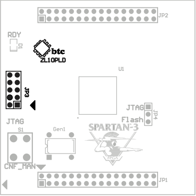
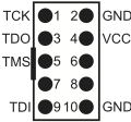
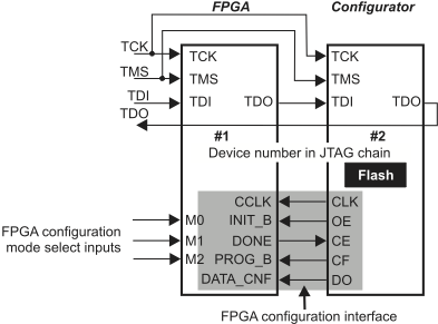
FPGA device and configuration memory (Flash memory U2) are connected to a JTAG chain, as in the below picture. This connection enables independent Flash memory programming and configuring of FPGA device with the use of programmer which is in accordance with Xilinx DLC III programmer (for example: ZL11PRG, ZL4PRG).
FPGA configuration mode selection
FPGA device, after turning on voltage, can be automatically configured (configuration is copied from Flash configuration memory) or can wait for configuration data which are supplied by the user with the use of JTAG interface. The choice of configuration mode takes place with the use of JP4 connector, according to the description, placed on the printed board.
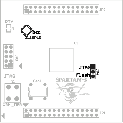
FPGA manual reconfiguration switch
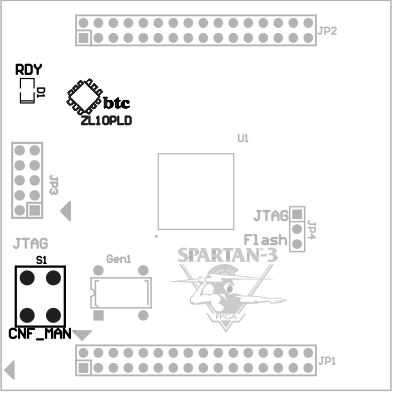
With the use of placed on the board button (its placement is shown in the below picture) the user in any moment can restore FPGA configuration which is saved in the memory. The correct FPGA configuration is indicated by RDY LED.
Quartz generator
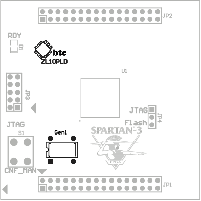
ZL10 PLD is equipped with quartz generator with 3.6864MHz output frequency and 5V power supply voltage. Thanks owing to the fact that the quartz generator is placed in the socket, the user can exchange it for any other, useful in application testing.
ZL9PLD base board peripherals connection
The ZL10PLD module is adapted to cooperation with ZL9PLD base board. On picture below is shown way of connection to module peripherals from ZL9PLD base board.
