ZL11AVR
From Kamamilabs.com - Wiki

Description
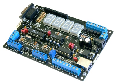
Development kit for AT90S1200/2313/ATtiny2313 microcontrollers. A board designed for building simple applications with AVR AT90S1200, AT90S2313 and ATtiny2313 microcontrollers. Its equipment, easy adaptation to personal requirements, as well as hardware compatibility with the AVT-3500 board make it suitable for both beginners and advanced users who want to work with microcontrollers or quickly build a microprocessor controller.

Basic feature and parameters
- ATtiny2313 microcontroller with flash memory programmed in the system - ISP (board is adapted to cooperate with microcontrollers AT90S1200, AT90S2313 and ATtiny2313),
- ISP connector for programming microcontrollers,
- built-in 4-digit, multiplexed LED display,
- possibility of using the LCD display with the controller compatible with HD44780 (e.g. LCD1602),
- microcontroller can be programmed using standard Atmel ISP programmers from Atmel and ZL20PRG programmer,
- built-in 4-channel, 8-bit A/D converter and 8-bit D/A converter (PCF8591),
- built-in precision reference voltage source with adjustable value,
- possibility of powering from USB or external power supply 9...12 VDC (built-in voltage converter),
- built-in RS232 interface (with voltage converter on MAX232 or transistors),
- microcontroller I / O port lines available on pin connectors,
- 2-button keyboard,
- configuration with a few jumpers
Standard equipmend
| Code | Description |
|---|---|
| ZL11AVR |
|
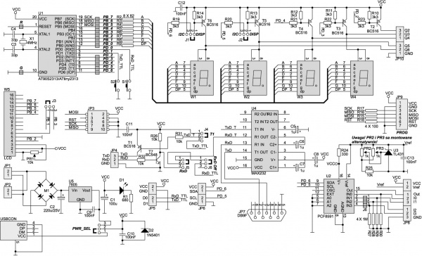
Electrical schematic

Placement of elements on the board
Connecting the LCD display to the microcontroller
Assignment of LCD module interface signals to the microcontroller pins:
| Output name of LCD | Output number of LCD | Port line name of AVR |
|---|---|---|
| RS | 4 | PB2 |
| E | 6 | PB1 or PB3 (see the table below) |
| D4 | 11 | PB4 |
| D5 | 12 | PB5 |
| D6 | 13 | PB6 |
| D7 | 14 | PB7 |
Selection of the signal controlling the E line of the LCD module (J3):
| Position | Designation on PCB | Signal E controlled from line... |
|---|---|---|
| 1-2 | PB1 | ...PB1 |
| 2-3 | PB3 | ...PB3 |
Connecting the LED display to the microcontroller
The way of connecting display segments to the microcontroller I/O line
| Segment LED | Line I/O |
|---|---|
| A | PB7 |
| B | PB6 |
| C | PB5 |
| D | PB4 |
| E | PB3 |
| F | PB2 |
| B | PB1 |
| DP (point) | PB0 |
The method of connecting amplifiers of common display cathodes to the microcontroller I/O line
| Display cathode... | Line I/O |
|---|---|
| ...W1 | PD6 |
| ...W2 | PD5 |
| ...W3 | PD4 |
| ...W4 | PD3 |
Jumper J1, J2, PWR_SEL function
J1 jumper function
| Position | Designation on PCB | Description |
|---|---|---|
| 1-2 | DISP | If PD6 controls W1 anode |
| 2-3 | I2C | If PD6 is SDA line |
J2 jumper function
| Position | Designation on PCB | Description |
|---|---|---|
| 1-2 | DISP | If PD5 control W2 anode |
| 2-3 | I2C | If PD5 is SCL line |
Selecting of power source (between USB and non-stabilized external power supply) can be made using the PWR_SEL jumper
| Position | Designation on PCB | Description |
|---|---|---|
| 1-2 | USB | Power supply from USB |
| 2-3 | EXT | Power supply from external 9...12 VDC |
RS232 interface
In the case of self-assembly of the board, one of two possible variants of the voltage interface should be selected. Because of reliability, an interface based on the MAX232 (U4) chip is recommended. In this case, you can not assemble elements: T1, R32 and J4.
Jumper J4, J5 and J6 are used to select the voltage interface (in case the user decides to install both of his versions on the board). The jumpers J4... 6 functions are shown below.
J4 jumper function
| Position | Designation on PCB | Description |
|---|---|---|
| 1-2 | Off | T1 base disconnected from line TxD_TTL (recommended position for MAX232 in RS232) |
| 2-3 | RS | T1 base connected to line TxD_TTL (recommended position for transistor voltage converter in RS232) |
J5 jumper function
| Position | Designation on PCB | Description |
|---|---|---|
| 1-2 | MAX | T7 collector disconnected from line RxD_TTL (recommended position for MAX232 in RS232) |
| 2-3 | T | T7 collector connected to line RxD_TTL (recommended position for transistor voltage converter in RS232) |
J6 jumper function
| Position | Designation on PCB | Description |
|---|---|---|
| 1-2 | - | Recommended position when T7 is not used as an input buffer |
| 2-3 | RxD Off | Recommended position when T7 is used as an input buffer and MAX232 is used in RS232 |
ISP programming
The microcontroller used in the board can be programmed using the ISP (In System Programming) programmer, for example ZL20PRG. There are two ISP connectors available:
- JP3, adapted to standard IDC10 connectors (ZL20PRG),
- JP9, enabling the use of any programmer equipped with one-contacts connectors.
Both connectors make possible to power ISP programmers with 5V voltage.
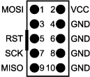
Placement of ISP signals on JP3 connector:

C/A and A/C converters
The standard equipment of the board is PCF8591, which integrates a 4-channel A/D converter (each channel with a resolution of 8 bits) and a D/A converter with a voltage output (also with a resolution of 8 bits). Access to the converters is possible via the I2C bus. The reference voltage for the converters is generated by the U3 chip. It is regulated with using PR3 potentiometer (or PR2, depending on the version).
Reset
Microcontroller used in the ZL11AVR board can be reset by the user with a jumper placed on the pins marked as G and R. Their short circuit reset the microcontroller.