ZL14PLD
From Kamamilabs.com - Wiki

Description
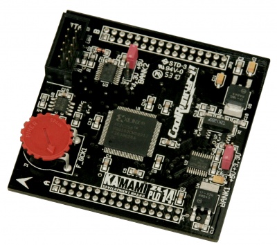
DipPLD module was developed to make easier common using of CPLD chips by constructors, which can not or will not invest in automated component mounting system of elements with small pitch (0.5mm).
Basic paremeters
- CPLD XC2C256 chip (256 macrocells) from CoolRunner-II family in VQFP100 package
- 16 lines with buffers adjusted to 5V signals
- Embedded clock frequency adjusted generator and oscillator 32.768kHz
- Module adapted to using with ZL15PLD board
Standard equipment
| Code | Description |
|---|---|
| ZL14PLD |
|
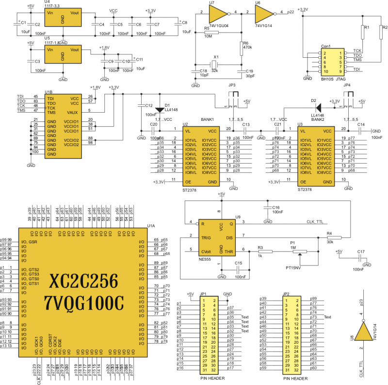
Electrical schematic
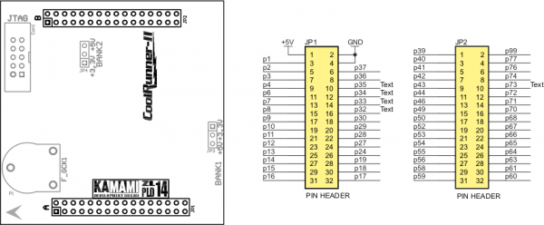
Position of the most important elements of module
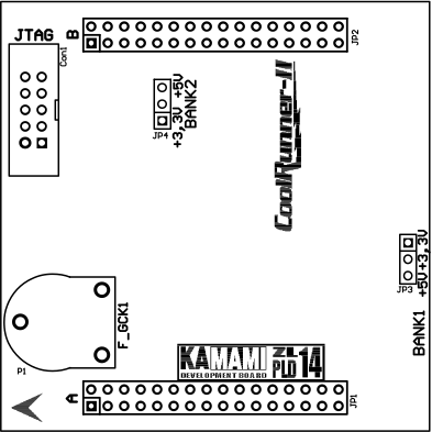
Module output description
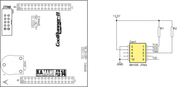
JTAG connector
Module is equipped with 10-pins IDC connector. To the connector can be connected programer/configurator ISP (e.g. ZL11PRG or ZL4PRG). Position of IDC connector and signals was presented on the picture below.
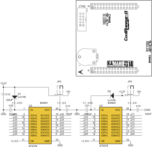
Buffers adjusted to the 5V signals
Module is equipped with two 8-pins buffers ST2378, which make possible to lead to the programmable chip 16 lines with signals 5V or 3.3V. Configuration of buffers depends on jumpers BANK1 (JP3) and BANK2 (JP4). Description of configuration was presented below.
| Signal level | I/O lines | Jumper configuration |
|---|---|---|
| 3,3 V | p28, p29, p30, p32, p33, p34, p35, p36 | BANK1 in position 3,3 V (1-2) |
| 5 V | p28, p29, p30, p32, p33, p34, p35, p36 | BANK1 in position 5 V (2-3) |
| 3,3 V | p68, p70, p71, p72, p73, p74, p76, p77 | BANK2 in position 3,3 V (1-2) |
| 5 V | p68, p70, p71, p72, p73, p74, p76, p77 | BANK2 in position 5 V (2-3) |
Clock signal sources
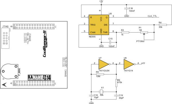
ZL12PLD module is equipped with two clock signal sources: oscillator 32.768kHz and adjusted clock generator based on 555 timer, which frequency can be controlled with potentiometer F_GCK1 (P1).
